Quantum technology is promising, but also perplexing. In the coming decades, it is expected to provide us with various technological breakthroughs: smaller and more precise sensors, highly secure communication networks, and powerful computers that can help develop new drugs and materials, control financial markets, and predict the weather much faster than current computing technology ever could.
To achieve this, we need so-called quantum materials: substances that exhibit pronounced quantum physical effects. One such material is graphene. This two-dimensional structural form of carbon has unusual physical properties, such as extraordinarily high tensile strength, thermal and electrical conductivity – as well as certain quantum effects. Restricting the already two-dimensional material even further, for instance, by giving it a ribbon-like shape, gives rise to a range of controllable quantum effects.
This is precisely what Mickael Perrin’s team leverage in their work: For several years now, scientists in Empa’s Transport at Nanoscale Interfaces laboratory, headed by Michel Calame, have been conducting research on graphene nanoribbons under Perrin’s leadership. “Graphene nanoribbons are even more fascinating than graphene itself,” explains Perrin. “By varying their length and width, as well as the shape of their edges, and by adding other atoms to them, you can give them all kinds of electrical, magnetic, and optical properties.”
Ultimate precision – down to single atoms
Research on the promising ribbons isn’t easy. The narrower the ribbon, the more pronounced its quantum properties are – but it also becomes more difficult to access a single ribbon at a time. This is precisely what must be done in order to understand the unique characteristics and possible applications of this quantum material and distinguish them from collective effects.

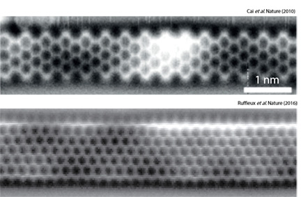
The extremely narrow ribbons with their atomically precise edge exhibit strong quantum effects, making them particularly interesting to researchers. Image: Empa
In a new study published recently in the journal Nature Electronics, Perrin and Empa researcher Jian Zhang, together with an international team, have succeeded for the first time in contacting individual long and atomically precise graphene nanoribbons. Not a trivial task: “A graphene nanoribbon that is just nine carbon atoms wide measures as little as 1 nanometer in width,” Zhang says. To ensure that only a single nanoribbon is contacted, the researchers employed electrodes of a similar size: They used carbon nanotubes that were also only 1 nanometer in diameter.
Precision is key for such a delicate experiment. It begins with the source materials. The researchers obtained the graphene nanoribbons via a strong and long-standing collaboration with Empa’s nanotech@surfaces laboratory, headed by Roman Fasel. “Roman Fasel and his team have been working on graphene nanoribbons for a long time and can synthesize many different types with atomic precision from individual precursor molecules,” Perrin explains. The precursor molecules came from the Max Planck Institute for Polymer Research in Mainz.
As is often required for advancing the state of the art, interdisciplinarity is key, and different international research groups were involved, each bringing in their own specialty to the table: The carbon nanotubes were grown by a research group at Peking University, and to interpret the results of the study, the Empa researchers collaborated with computational scientists at the University of Warwick. “A project like this would not be possible without collaboration,” Zhang emphasizes.
Contacting individual ribbons by nanotubes posed a considerable challenge for the researchers. “The carbon nanotubes and the graphene nanoribbons are grown on separate substrates,” Zhang explains. “First, the nanotubes need to be transferred to the device substrate and contacted by metal electrodes. Then we cut them with high-resolution electron-beam lithography to separate them into two electrodes.” Finally, the ribbons are transferred onto the same substrate. Precision is key: Even the slightest rotation of the substrates can significantly reduce the probability of successful contact. “Having access to high-quality infrastructure at the Binnig and Roher Nanotechnology Center at IBM Research in Rüschlikon was essential to test and implement this technology,” Perrin says.
From computers to energy converters
The scientists confirmed the success of their experiment through charge transport measurements. “Because quantum effects are usually more pronounced at low temperature, we performed the measurements at temperatures close to absolute zero in a high vacuum,” Perrin explains. But he is quick to add yet another particularly promising quality of graphene nanoribbons: “Due to the extremely small size of these nanoribbons, we expect their quantum effects to be so robust that they are observable even at room temperature.” This, the researcher says, could allow us to design and operate chips that actively harness quantum effects without the need for an elaborate cooling infrastructure.

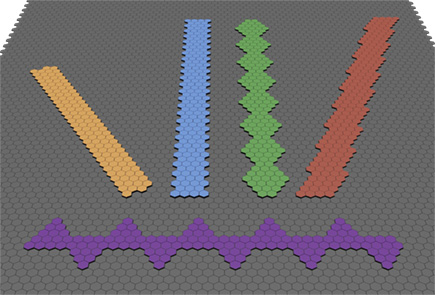
The properties of nanoribbons vary depending on their width and the shape of their edges. Image: Empa
”This project enables the realization of single nanoribbon devices, not only to study fundamental quantum effects such as how electrons and phonons behave at the nanoscale, but also to exploit such effects for applications in quantum switching, quantum sensing, and quantum energy conversion”, adds Hatef Sadeghi, a professor at the Univeristy of Warwick who collaborated on the project.
Graphene nanoribbons are not ready for commercial applications just yet, and there is still a lot of research to be done. In a follow-up study, Zhang and Perrin aim to manipulate different quantum states on a single nanoribbon. In addition, they plan on creating devices based on two ribbons connected in series, forming a so-called double quantum dot. Such a circuit could serve as a qubit – the smallest unit of information in a quantum computer. Moreover, Perrin, in the context of his recently obtained ERC Starting Grant and an SNSF Eccellenza Professorial Fellowship, plans to explore the use of nanoribbons as highly-efficient energy converters. In his inaugural lecture at ETH Zurich, he paints a picture of a world, in which we can harness electricity from temperature difference, while hardly losing any energy as heat – this would indeed be a real quantum leap.
International collaboration
Multiple research groups made key contributions to this project. The graphene nanoribbons were grown by Empa’s nanotech@surfaces laboratory, headed by Roman Fasel, based on precursor molecules provided by the team of Klaus Müllen from the Max Planck Institute for Polymer Research in Mainz. The nanoribbons were integrated into nanofabricated devices by members of Empa’s Transport at Nanoscale Interfaces laboratory, headed by Michel Calame, in which Mickael Perrin’s group is embedded. The precisely-aligned, high-quality carbon nanotubes required for this particular study were provided by the research group of Jin Zhang at Peking University. Finally, to interpret the results of the study, the Empa researchers collaborated with computational scientists at the University of Warwick under the supervision of Hatef Sadeghi.
Prof. Dr. Mickael Lucien Perrin
Transport at Nanoscale Interfaces
Phone +41 58 765 46 10
mickael.perrin@empa.ch


